Hannu-Pekka Komsa homepage
Assistant Professor at University of Oulu
2D materials
Defects in 2D materials, imaging and damage in electron microscope.
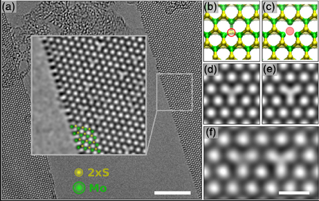
Left: Transmission electron microscope image of MoS2 showing a large concentration of sulfur vacancies (and a crack in the middle) produced by the beam. Both single and double vacancies are observed.
H.-P Komsa et al., Phys. Rev. Lett. 109, 035503 (2012)
H.-P. Komsa et al., Phys. Rev. B 88, 035301 (2013)
Y.-C. Lin, Nature Comm. 6, 6736 (2015)
E. Sutter, Nano Lett. 16, 4410 (2016)
V. Vierimaa, Nanoscale 8, 7949 (2016)
R. Ibragimova, Nanoscale Adv. 3, 1934 (2021)
Optical properties of 2D materials.
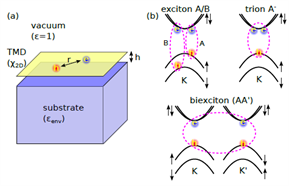
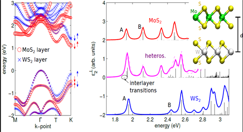
Left: Electronic structure and optical absorption spectrum of MoS2/WS2 bilayer hetero-structrure. The states are colored according to the projection to each layer. The optical spectrum behaves as the sum from the monolayers. Optically inactive interlayer exciton are found below the absorption edge.
H.-P. Komsa et al., Phys. Rev. B 88, 085318 (2013)
Above: Trions and biexcitons in 2D materials calculated using a combined DFT+quantum Monte Carlo approach.
I. Kylänpää and H.-P. Komsa, Phys. Rev. B 92, 205418 (2015)
MXenes, surface composition and properties.
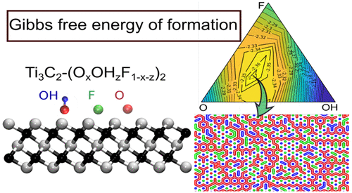
Left: Composition and distribution of O, OH, and F functional groups on the surface of Ti3C2 MXene: Gibbs free energy map and the atomic structure for the minimum energy composition. Calculated via Monte Carlo simulations on cluster expansion model fit to DFT energies.
R. Ibragimova et al, ACS Nano 13, 9171 (2019)
R. Ibragimova et al., J. Phys. Chem. Lett. 12, 2377 (2021)
Raman spectroscopy
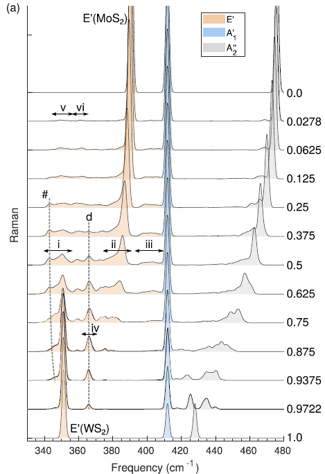
Simulations of Raman spectra.
Right: Simulated Raman spectra of (Mo,W)S2 alloy. We developed efficient method for simulating Raman spectra of defective system, which makes use of the projections of the supercell vibrational modes to those from pristine unit cell and the Raman tensors from pristine system calculated using DFT.
A. Hashemi et al., Phys. Rev. Mat. 3, 023806 (2019)
Z. Kou et al., npj Comput. Mater. 6, 59 (2020)
P. Sutter et al., Nano Today 37, 101082 (2021)
E. Berger et al., J. Mater. Chem. C 11, 1311 (2023)
Raman spectra database from high-throughput calculations.
Website, manuscript
3D materials
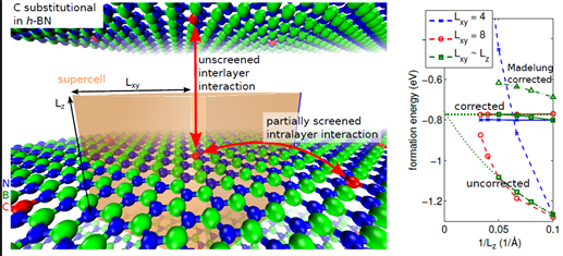
Left: Calculations of charged defects located at surfaces or interfaces within the supercell approach suffer from a strong and anisotropic spurious electrostatic interactions between the charge and its periodic images.
We have developed an a posteriori method for correcting the energetics. It was also applied to defects in 2D materials.
H.-P. Komsa et al., Phys. Rev. Lett. 110, 095505 (2013)
H.-P. Komsa et al., Phys. Rev. X 4, 031044 (2014)
We have developed an a posteriori method for correcting the energetics. It was also applied to defects in 2D materials.
H.-P. Komsa et al., Phys. Rev. Lett. 110, 095505 (2013)
H.-P. Komsa et al., Phys. Rev. X 4, 031044 (2014)
Right: We have studied the role of defects for the properties of CIGS (CuInGaSe2) solar cell material.
Right: 3D printed atomic structure of CuInSe2, which was used in the cover of Advanced Electronic Materials special issue on Aalto University Materials platform.
M. Malickaya et al., Adv. El. Mat. 3, 1600343 (2017)
M. Malickaya et al., J. Phys. Chem. C 121, 15516 (2017)
Right: 3D printed atomic structure of CuInSe2, which was used in the cover of Advanced Electronic Materials special issue on Aalto University Materials platform.
M. Malickaya et al., Adv. El. Mat. 3, 1600343 (2017)
M. Malickaya et al., J. Phys. Chem. C 121, 15516 (2017)
1D materials - atomic chains
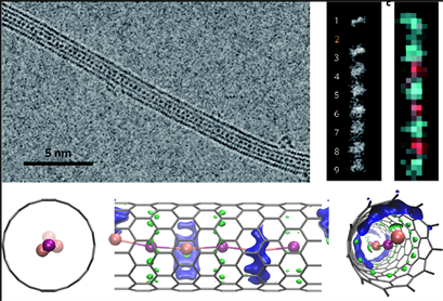
Left: Scanning transmission electron microscope image of a one-dimensional ionic chain, i.e., a one-dimensional salt, inside carbon nanotube. Electron energy loss mapping can be used to distinguish the two ions.
According to calculations the Cs ions are attracted to the nanotube walls while I ions are confined at the center. This also leads to different dynamic behavior of the two ions.
R. Senga et al., Nature Mater. 13, 1050 (2014)
H.-P. Komsa et al., Nano Lett. 17, 3694 (2017)
PR: Ars Technica, nanotechweb.org,
Tekniikka&Talous (in finnish)
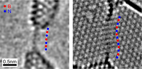
Right: Atomic chains can also be crafted under electron beam via continuous thinning of nanoribbons, which in turn are created by drilling holes to the 2D material. When such process was applied to single layer BN, chains exhibiting alternating B and N atoms were observed.
O. Cretu et al., ACS Nano 8, 11950 (2014)
O. Cretu et al., ACS Nano 8, 11950 (2014)
0D materials

Materials Project database was screened for finding 0D materials, i.e., molecules that are van der Waals bonded and have high melting point. Their suitability for electronics applications was also investigated.
M. Bagheri and H.-P. Komsa, Adv. Electron. Mater 9, 2200393 (2023)
M. Bagheri and H.-P. Komsa, Adv. Electron. Mater 9, 2200393 (2023)


